20 Mar 2023
Introduction
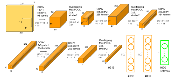
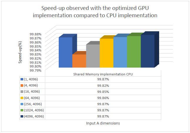
AlexNet is a popular convolutional neural network architecture designed by Alex Krizhevsky, Ilya Sutskever, and Geoffrey Hinton. AlexNet won the ImageNet Large Scale Visual Recognition Challenge (ILSVRC) in 2012 and significantly outperformed previous state-of-the-art methods. The architecture consists of 5 convolutional layers, 3 fully connected layers, and an output layer. In this report, I will compare the implementation of the convolutional layers and the matrix multiplication in the fully connected layers of AlexNet on a CPU and a GPU. The GPU implementation of Convolutional Layer achieved an average speed up of 99.458% compared to the CPU implementation. For the Matrix Multiplication implementation, the optimized GPU implementation gains an average speed up of 99.86% compared to CPU implementation.
Convolutional Layer
Comparison between CPU and GPU implementations
I implemented the convolutional layers of AlexNet on both CPU and GPU. The GPU used for the implementation is Nvidia Volta V100. An important feature of Volta V100 GPU includes configurable 96KB shared memory. I have used this shared memory and constant memory features of CUDA to optimize the GPU implementations of both Matrix Multiplication and Convolution. With the use of shared memory, the implementation of Convolutional Layer attains an average occupancy of 96% per SM.
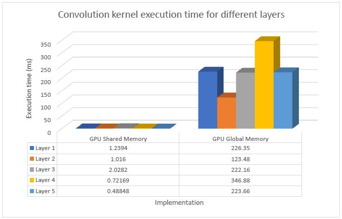
The naïve CPU implementation is taken in which the computation of each element of the output is carried out sequentially for all the different channels of the filters. This takes on average 3.266 seconds to complete for each layer. Compared to this, the optimized GPU implementation on average takes only 1ms to complete with 0 errors. The graph below depicts the execution time taken by GPU and CPU for different layers in seconds.
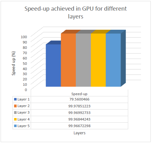
The speedups achieved by the GPU implementation of different layers on AlexNet can be seen in the graph below.
Basic GPU implementation
My initial implementation of the Convolutional layers on the GPU utilized the global memory to store the inputs and filters for the convolution operation. The implementation was not parallelized across channels and the number of threads was decided based upon the number of output elements to be computed. The basic idea was to assign the task of computation of one output pixel to a single thread for all the channels of input. This was a very naïve approach was taken basically taken from the CPU implementation of the convolutional layers.
For the optimization of this naïve approach, I decided to exploit the input and feature reuse with the 3D convolution operation. The input is reused for each batch of the filter and the filter is reused by each batch of the input. Here since the computation only takes place for a single batch, it was more effective to put the input in the shared memory as it will be used by all the filters. For further update, one can even put each layer of filter in the shared memory.
I also exploited the fact that the bias is necessarily constant and does not change throughout the runtime. Therefore, it is a perfect candidate to be put in the constant memory. The filter cannot be put in the constant memory due to restricted space in the constant memory.
Optimized GPU implementation with Shared Memory
The shared memory implementation also parallelises across the channels of the input. Convolution between each channel of the filter and the corresponding filter is stored in the thread registers and eventually an atomicAdd() operation is used in order to compute the sum of each of the thread’s output for an input channel. The atomicAdd() operation add additional overhead but the gain in speedup is considerable as compared to the naïve global memory-based implementation in GPU as can be seen from the graph below.
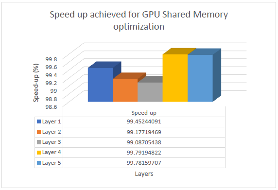
The Optimized GPU implementation gains average speed up of 99% compared to the GPU global memory-based implementation. The speed up gained in case of each of the layers can be seem in the graph below.
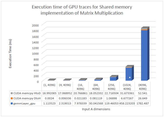
The GPU traces for different kernels and cudaMemcpy() in case of optimized GPU shared memory-based implementation is seen in the graph below.
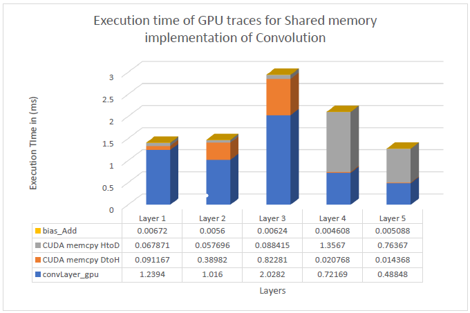
The bias_Add kernel is used to add the bias value to each of the output elements after the convolution results are outputted. The reason to employ a separate bias_Add kernel are specific to the loading and accessing of input data in the shared memory. The input data is loaded in form of strips of tiles of size tileW = BLOCK_SIZE + fShape.width – args.strideW and tileH = BLOCK_SIZE + fShape.width – args.strideH. The dimensions of the block, therefore, are (tileW, threadsPerSubblock), where threadsperSubblock decides the number of rows which are to be loaded in one strip of the tile. The thread blocks load strips of their tiles of size tileH*tileW one by one and put that into their shared memory. This process for a tile is sequential. To access the elements of shared input one must do this sequential retrieving which makes addition of the bias complex. With the experiments I conducted, the bias was getting added multiple times to a single element of output. To avoid this confusion altogether, I assigned the task of adding bias to a different kernel.
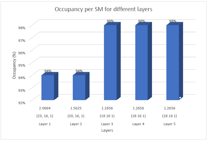
The occupancy of the optimized GPU implementation calculated by CUDA-Occupancy-Calculator is shown in the graph below for different layers with the initial respective Block Size and shared memory usage. The current implementation has a very good occupancy of 96% on average for all the layers.
Matrix Multiplication
Matrix multiplication is a fundamental operation in deep learning, and it is used extensively in convolutional neural networks (CNNs). AlexNet uses matrix multiplication in its fully connected layers. In this report, we will compare the implementation of matrix multiplication for the fully connected layers of AlexNet on a CPU and a GPU. We implemented three different versions of the GPU implementation: an unoptimized global memory-based implementation, an unoptimized unified virtual memory-based implementation, and a shared memory-based optimized implementation.
Comparison between CPU and GPU Implementations
The CPU implementation of Matrix Multiplication does use the concept of tiling, i.e, a tile of the output element is computed by adding the partial sums of matrix multiplication of tiles of the inputs A and B. This however done one tile of the output at a time hence there is a great scope of parallelization. Each of the individual tiles of the output can be computed by a block of size (args.tileW, args.tileH). This is implemented in a basic GPU implementation of the algorithm. The graph comparing the time taken by GEMM kernel for both the approaches can be seen below:
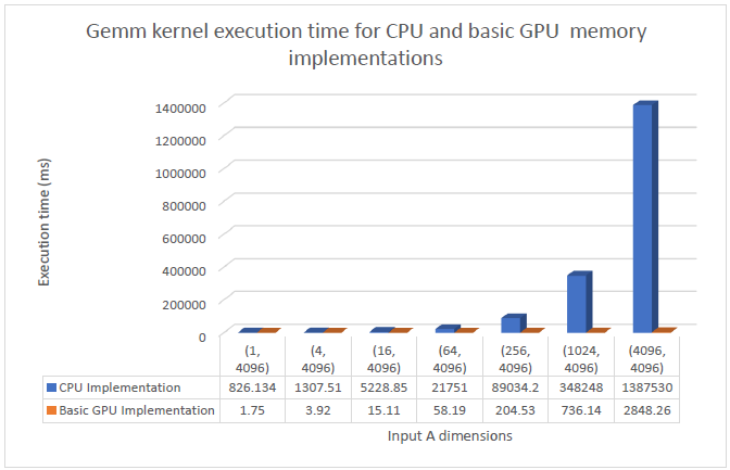
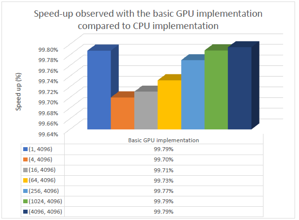
It can be observed that even the unoptimized implementation on the GPU significantly outperforms the CPU. The speed ups observed can be seen the graph below.
Basic GPU implementation with Unified Virtual Memory
Unified Memory is a single memory address space accessible from any processor in a system. The unified memory alleviates the usage of cudaMemcpy() completely the GPU can get the data directly from the CPU through page faults. For the next part of my implementation, I used Unified Virtual Memory in order to transfer data from the host to the device. The graph depicting the performance of GEMM kernel of the UVM based GPU implementation and the basic GPU implementation with the usual cudaMemcpy() is given below.
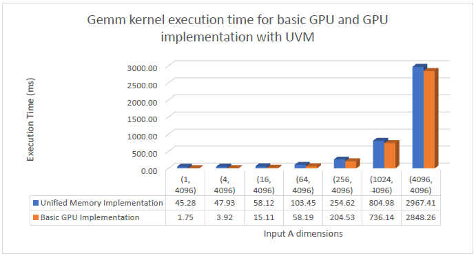
It can be observed that the use of UVM adds on additional overheads in the migration of the data to the device from the host. This can be observed in the graph above. In case of (1, 4096) Input A dimension, the additional overhead increases the execution time a lot. The migration overhead in this simple code is caused by the fact that the CPU initializes the data, and the GPU only uses it once. The overhead can reduce if the data is initialized on the GPU itself.
Optimized GPU implementation with Shared Memory
In the Optimized GPU implementation of matrix multiplication, the tiles of input A and input B are stored in the shared memory. The threads of each thread block co-ordinate to store the elements of their individual tiles in the shared memory. This approach offers significant performance improvement compared to the basic implementation where the inputs are stored in the global memory. The graph below shows the performance of the GEMM kernel for the global memory based and shared memory-based implementations.
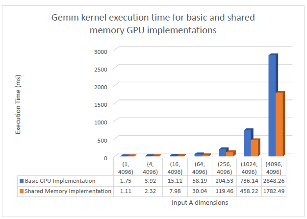
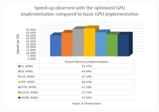
As the batch size scales, the shared memory approach shows considerable improvements over the basic global memory-based approach. The speedup gained by implementing the matrix multiplication in the shared memory can be seen in the graph below.
The stacked bar graph depicting the performance of the optimized GPU implementation is shown below.
Conclusion
The convolutional layers and matrix multiplication layers are implemented in GPU with optimization include use of shared/constant memory. The implementations gain considerable speed-up compared to the CPU implementations.
30 Dec 2022
Introduction
Load value locality is the concept of recurring values over time from particular static load instructions. If a load can be identified as consistently returning the same value, the CPU can exploit this pattern by predicting the result before the load instruction even executes, thus saving time and potentially memory bandwidth. Such value speculation is like branch prediction except with a whole word instead of one bit. Methods are required to verify load value predictions and also to correct mispredictions. In this report, we review prior work on load value prediction, discuss our designs and experiments to implement the concept in gem5, and examine our statistical results measuring rates of locality and final performance changes. The implementation for this project can be found on this repository.
The benefit of value locality is two-fold: First, the early availability of predicted load values enables dependent instructions to execute sooner and, second, accurate predictions relieve the memory system from fetching redundant data. In 1995, the first of these concepts was introduced to perform loads very early and verify in parallel to achieve zero-cycle loads in some cases Aus95. The second concept is that the CPU can bypass the data caches altogether, thus acquiring data that may not even exist in cache. Both concepts were explored in the seminal paper on value locality from 1996. Their basic structures were the load value prediction table (LVPT), load classification table (LCT), and constant verification unit (CVU) Lip96. The LVPT caches prior loaded data values. When it predicts a value, it forwards it to younger instruction. The LCT classifies the confidence as “unpredictable”, “predictable”, or “constant”. In the first two cases, the load must execute fully on data cache, then compare the true load value with the prediction. If correct, the LCT increases its confidence; otherwise, it decreases. “Constant” loads do not access memory at all. In 1998, researchers noted that mispredictions do not require all younger instructions to squash, but only those with directly-dependent data Bur98. Unfortunately, this selective squashing technique was considered too hard at the time Pai98. Other methods to increase prediction accuracy included tracking prediction history and using statistical inference.
Implementation details
1. Load Value Prediction and Classification Table
It was unnecessary to have separate LVPT and LCT tables, due to the only additional payload being the data stored in the LCT. The new table LVPCT contains all the functions that were implemented in their respective objects. These functions include: lookup, using an instruction address to identify a classification and corresponding value; upgrade/downgrade classification, which updates the LVPCT based on whether the value matches the current value and modifying the classification. The structure of an LVPCT entry looks like this:
| TID |
Classification (Can be Unpredictable 1, Unpredictable 2, Predictable or Constant) |
Value (uint64_t) |
No valid bit is required as the entries marked with Unpredictable 1 and 2 are considered invalid. The table has 1024 entries and is direct-mapped without tags.
2. Constant Verification Unit
The CVU is implemented as specified in the original paper. The replacement policy used is FIFO. It is hardcoded with 32 entries, since the constant loads will be few. The complexity of a CAM search could not be coded so we chose a simpler structure, a vector. These functions were included: insertConstantLoad, checkForStore, checkForConstantLoad, and isFull, which inserts the constant load into CVU, checks for presence of a store’s data address in CVU, and checks for the presence of an executed constant load for validation purpose. The checkForStore also invalidates entries in the CVU, which entails entry deletion. The structure of a CVU entry looks like this:
| TID |
Data Address |
Index in the LVPCT table |
3. Forwarding and Verification
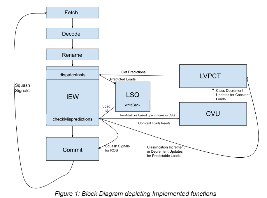
In the dispatch stage, the load gets its classification using lookup on the LVPCT table. The value from the table is copied into the destination register. The instruction is, then, inserted into the instruction queue with LSQ::insertLoad and the dependent instructions are notified of the available value. To notify dependents, we follow the pattern of existing dependence-management code with some modifications (see InstructionQueue::wakeLoadDependents). The dependent instructions are removed from a waiting queue (or dependency graph) and the corresponding register scoreboard entry is marked as ready. Thus, the predicted value is forwarded early. The purpose of “value forwarding” in our context is to send predicted load values to dependent instructions early on in execution, such that dependent instructions can operate sooner than they otherwise would have.
To verify predictable loads, it needs to execute normally in the LSQ and get the true value from memory. The verification is done by IEW::checkMisprediction called in LSQUnit::writeback (see Fig.1). Once the true value writes-back to the destination register, it is compared with the predicted value. If they are equal, then the load commits normally. If they are unequal, the load still commits normally as the value for the load is corrected by usual execution of LSQUnit::executeLoad. All subsequent instructions, though, are squashed. We achieve this squashing by marking the instructions as a false branch prediction and allowing the branch squashing mechanism to operate. It is not necessary to squash mispredicted predictable loads because they are self-correcting after the writeback stage.
Constant loads, however, cannot be corrected in this same way because they are supposed to skip the memory system altogether. Thus, mispredicted constant loads must be squashed along with all subsequent instructions. Constant loads are verified in the writeback stage by checking the CVU for existence of a matching entry (see earlier section on CVU). If a match is found, then it commits normally. Otherwise, it must squash. We have had many difficulties making constant load verification successful. See the appendix for more details on this. The CVU is kept coherent with memory by invalidating entries whose data address matches incoming stores.
Benchmarks
The benchmarks used to evaluate the LVPT were the following: deep sjeng, lbm, leela, mcf, imgick. Unfortunately bwaves could not run on the x86 system (segmentation fault). So, we replaced it with leela. We evaluated the implementation with the number of cycles for the benchmark. It can be identified whether the LVPT is optimizing the O3 processor based on the improvement in number of cycles. In addition, metrics involving the unit’s prediction quality were correctly/incorrectly predicted values, and time spent within each classification.
Results
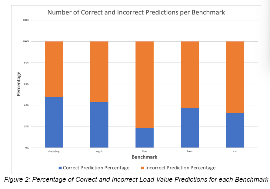
The figure 2 demonstrates the accuracy of the LVPT, with higher percentages the unit is able to upgrade an instruction to a “constant” classification where its value can be forwarded effectively. Unfortunately as seen in lbm we are seeing higher percentages of incorrect predictions, 80%, therefore it can be deemed to take longer to reach said level as it will thrash between “unpredictable” states. However, for the other benchmarks we are seeing percentage levels of near 40% to 50% which is significantly better than lbm. For these benchmarks, the data is more predictable and could be optimized better than the rest.
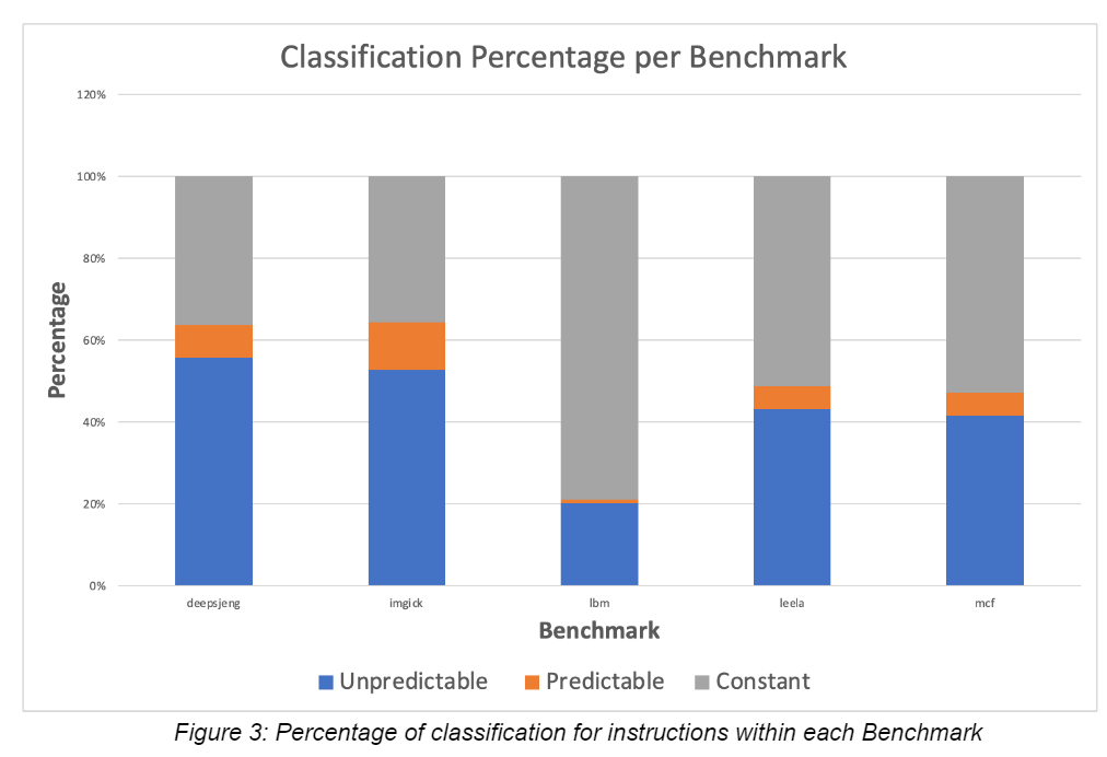
The figure 3 above shows that during the run of each benchmark the “unpredictable” state was the most seen state for the load instructions. What this represents is that the behavior for each instruction is thrashing between values and a result cannot be considered constant for more than 50% of the time. While for the lbm benchmark it was clear that there was a significant difference comparatively where the majority of the instructions were held at constant. This figure provides insight on how much work could have been optimized in relation to each benchmark. Benchmarks with a high percentage of “constant” are expected to see higher possible improvements to execution.
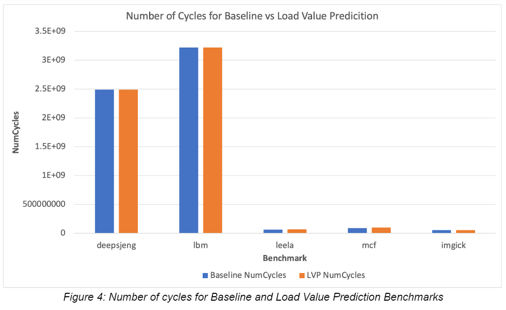
The figure 4 demonstrates the optimization done by the Load Value Prediction Unit for each benchmark. There is minimal optimization to the benchmarks; this is due to the inability to accurately predict constant values. As discussed before this hinders the unit’s ability to fully optimize the processor. Some of the number of cycles are larger with the LVPT due to numerous incorrect predictions. However, with the prediction for “predictable” loads, the figure 4 accurately displays slight optimizations and reductions in the number of cycles. Therefore the data provides inconclusive results on how effective the load value prediction unit is with the selected benchmarks.
Conclusion
Based on our working implementation of predicting load value, it would be seen that the simulations took very short time due to early forwarding of values. The squashing in case of misprediction of predictable loads was also performed effectively leading. In case of constant loads, the performance could not be observed even after rigorous testing of our approach due to a core dump. More on that can be read about in the appendix.
Appendix
Constant Load Prediction
The value prediction for the Constant Loads is conducted in the same way as that of the Predictable loads. The dependent instructions are removed from a waiting queue (or dependency graph) and the corresponding register scoreboard entry is marked as ready. Thus, the predicted value is forwarded early.
For Constant Loads the checkMispredicton function calls the badConstantLoadPrediction function which verifies whether a constant load exists in the CVU or not. Furthermore, when the LSQ executes a store instruction, it searches for matching data addresses in the CVU and invalidates all found entries.
We were unable to successfully figure out how to bypass the memory. We tried several methods including bypassing the LSQUnit::initiateAcc method in the LSQUnit::executeLoad method in LSQ and the completeAcc call in LSQ::writeBack. We also tried preventing constant loads from being inserted into the LSQ at all, but this caused problems with the load instruction never reaching the verification stage or commit. We tried spoofing constant load execution by allowing them to complete in memory and then restoring the prediction afterward. At least then, we could determine if the verification logic was correct.
- Squashing on Misprediction
We tried squashing the instructions using the squashDueToMemOrder methods in IEW stage. Function squashDueToMemOrder squashed both the load instructions and the dependents. This resulted in the program hanging because of bad squashing. We next tried to test using the squashDueToBranch which does not squash the load instruction but only the dependents. In order to do so, we provided the correct value to the load instruction using the getStashedValue method of DynInsts and then used squashDueToBranch. This caused a Core Dumped error with the fault “Tried to execute unmapped address 0”.
29 Dec 2022
Introduction to Deep Double Descent
The phenomenon of deep double descent was first postulate by Belkin et. al(2018). Belkin worked with the
neural network and observed that when one increases the width of a network(i.e., increase number of
neurones), the test error appears to increase for a range of width and then decreases and saturates. This
observation was reported continuously for different kinds of network architectures by even the predecessors
of Belkin including Opper (1995; 2001), Advani & Saxe (2017), Spigler et al. (2018), and Geiger et al.
(2019b).
The reason behind such an increase and then, decrease in the test error can be understood by combining two
conventional thought processes for the question ‘Whether larger models are better or worse?’. The two
conventional viewpoints can be understood as such,
- Bias Variance trade-off - The bias is a measure of how well the data performs on training dataset, whereas,
the variance is a measure of how well the model performs on test dataset given it trained upon a given
training dataset. The concept of Bias-Variance trade off is a fundamental concept of classical statistical
theory. According to the concept, after certain threshold width, the model starts to ‘overfit’ the training
dataset hence it performs poorly on the test data and it’s generalisation capability decreases. Therefore the
understanding is that the ‘larger models are worse’.
- The modern neural networks do not exhibit any such circumstance. The larger models have more
parameters hence are able to fit even random labels. Hence, the understanding becomes that ‘larger models
are better’.
The double descent is not only observed in case of varying model width but also in case of varying number
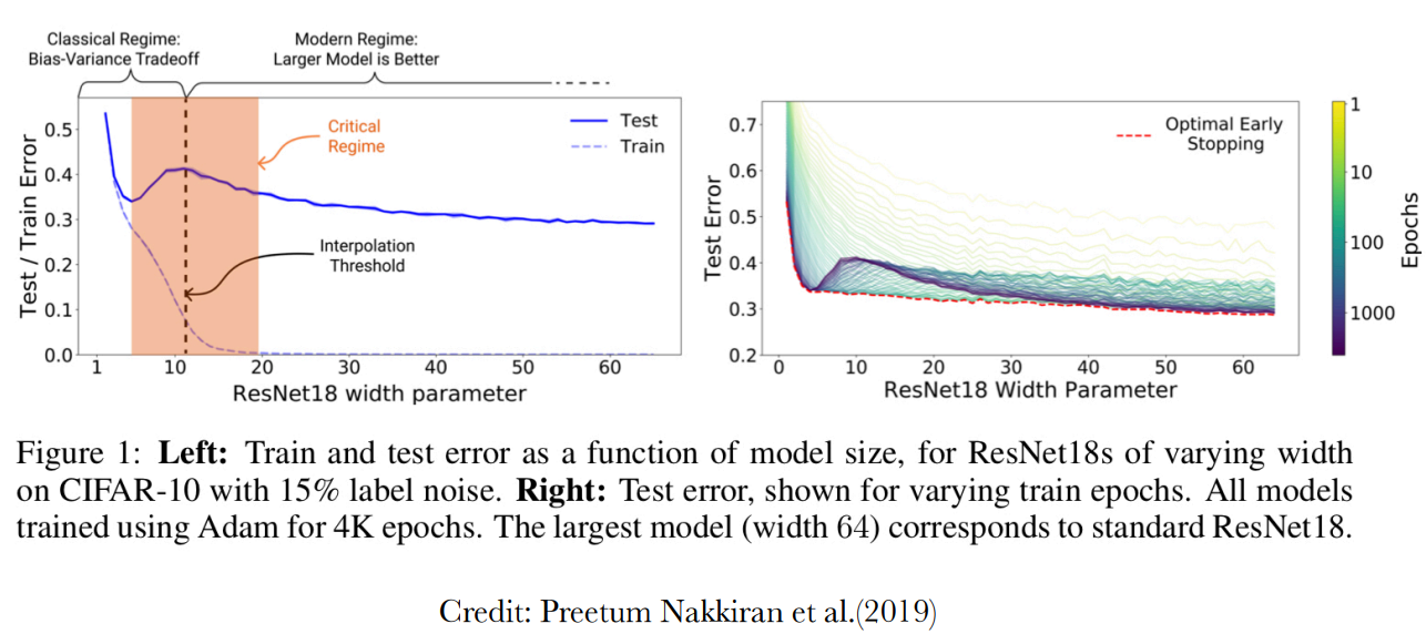
of epochs as discussed in the paper by Preetum Nakkiran et al.(2019). The paper also describes a measure of
complexity of model called effective model complexity and describes in detail the regions of the width versus
test error graph as shown in figure 1.
Experimental Setup
Dataset
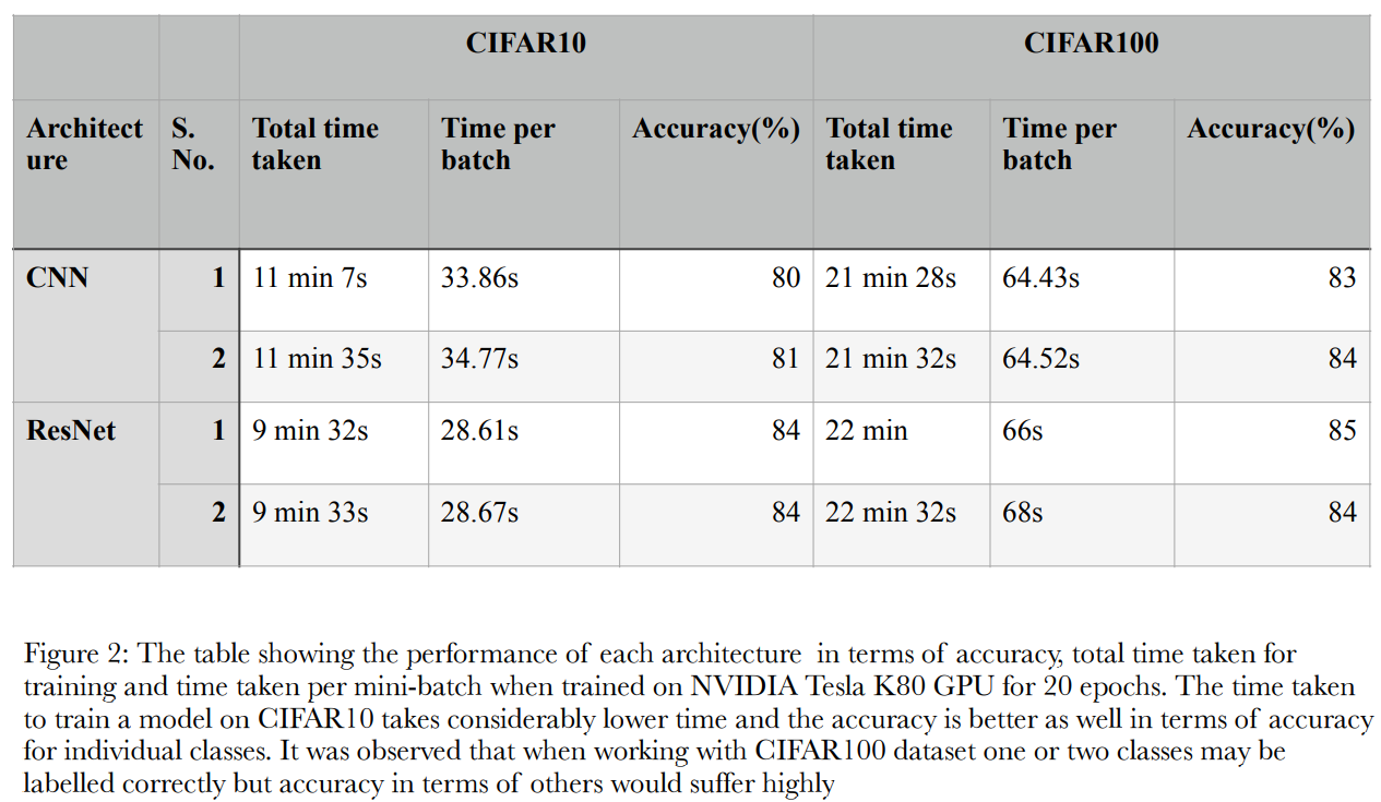
A study was conducted initially to understand which dataset to work with considering the training time taken
to train upon CIFAR10 and CIFAR100. Run times were compared for the required architectures with
CIFAR10 and CIFAR100. It was observed that working on CIFAR10, gives better results in terms of time
and accuracy considering it has 10 classes. The performance on CIFAR100 data proved to be comparable to
that on CIFAR10 in terms of runtime but accuracy suffers as it has 100 classes.
Note: Originally, in the paper by Preetam Nakkiran et al.(2019), the model was trained with Adam Optimiser for
4000 epochs. At the current speed of training, training CNN on CIFAR100 for 4000 steps would take 15 hours
approximately.
Architecture
Two of the architectures tested upon are based on the architectures used in the paper by Preetum
Nakkiran(2019), where as, BCNN were added in the later part of the study. The following are the
architectures considered:
- Convolutional Neural Network - The CNN5 was used with layer width parameter as c, where the layer
width varies [c, 2c, 4c, 5c] for the Convolutional layers. It was observed the base line model with c equal
to 60 gives 80% accuracy on the CIFAR10 dataset.
- Residual Neural Network - The ResNet18 architecture was employed with each ResNet block has it’s
width varying in the same fashion i.e, [c, 2c, 4c, 8c] for the Convolutional layers.
- Binarised CNN - The BCNN was introduced later in the study to try and observe the interpolation
effect(double descent) phenomenon. The basic structure of network is exactly the same as that of CNN5
but with quantised convolutional layers introduced. Also, the BCNN unlike CNN5 is trained using Keras,
not Pytorch.
Number of Epochs
The models of CNN and ResNet architectures are all trained for 40 epochs and mini-batch size of 128 due
to computational constraint as only Google Colab’s Tesla GPU was used. The random seed of 0 is added in
order to make sure the output remains constant for a value of c. It was still observed that there was certain
variability between the values of test error obtained for each width parameter value.
BCNN on the other hand has been analysed for two cases epoch 40 and epoch 400, as training of BCNN is
considerably faster than CNN5. Understandably so, it is because of the better memory utilisation and use of
bit wise operations instead of arithmetic ones that are used in CNN5. For better understanding, kindly refer
to the paper [2] by Benjio et al.
Optimization
The standard adam optimiser is utilised with a learning rate of 10-4 for all the architectures.
Regularisation
No regularisation technique was utilised. Further study is required to see the impact of regularisation upon
double descent phenomenon.
Experiments and Results
The main objective of each experiment conducted is to observe the interpolation phenomenon in CNN5,
ResNet18 and BCNN. The experiment conducted in case of each architecture is explained below,
CNN5
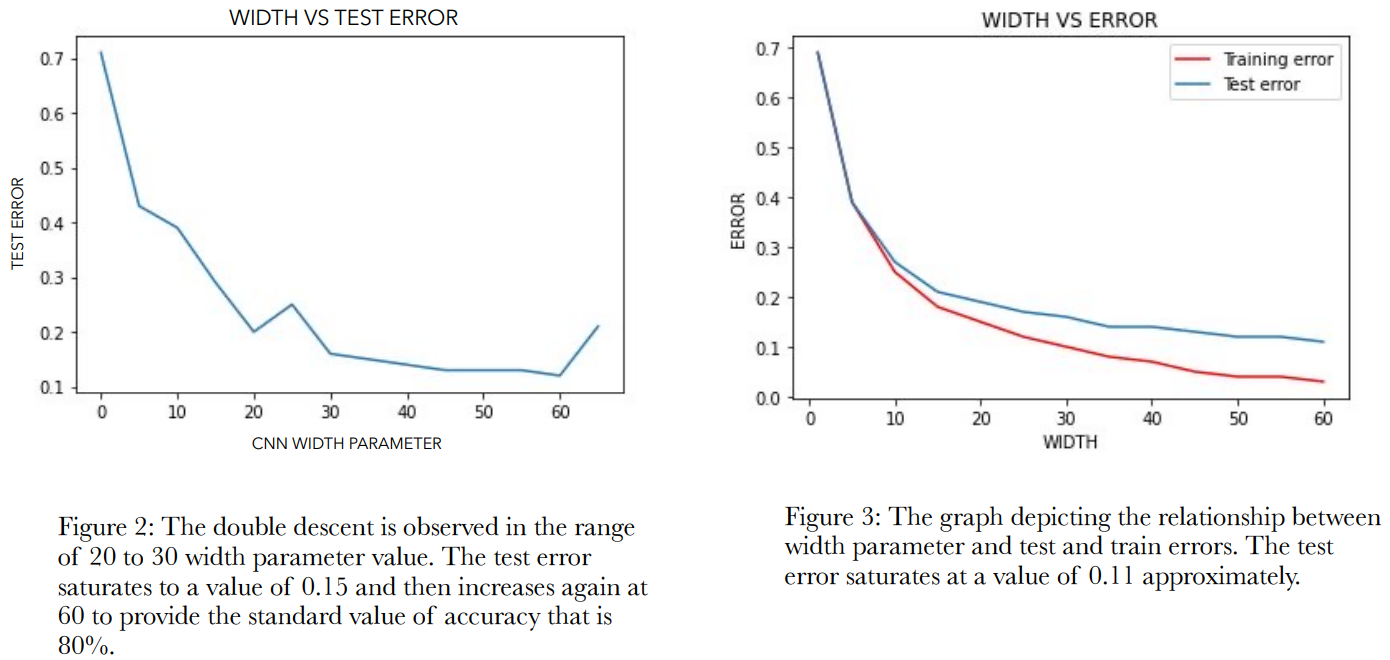
The Pytorch platform was used in order to try and observe the double descent phenomenon after the plotting
of test errors for values of width parameter c. The c values were chosen at an interval of 5, starting with 1,
up till 65. For each of c values the test error and train error attained, is plotted on the graph. Double descent
phenomenon was observed only in one out of five tries with the complete width value set. There was greater
variability between each experiment try result. And nothing could be predicted conclusively with respect why
such a thing is happening, as double descent issue should be observed in all tried. It was however assumed
that this issue may be due to the fact that the model is trained for very less number of epochs(40 epochs) due
to the computational constraint. However, it was observed that the test error while trying to approach zero,
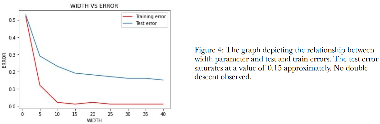
saturates near the value of 0.15(15%) test error as can be seen in the Figure 2.
ResNet18
The Pytorch platform was used in order to try and observe the double descent phenomenon after the plotting
of test errors and train errors for values of width parameter c. The c values were chosen at an interval of 5,
starting with 1, up till 40. For each of c values the test error and train error attained, is plotted on the graph.
There was no instance where double descent presented itself out of the 7 trials made. The graph showing
width parameter on the x axis and the test and train errors on the y axis for one of the trials can be observed
in figure 4 given
BCNN
There are two experiments conducted with respect to Binarise CNN. The experiment unlike the previous
ones before is conducted on Keras instead on Pytorch. The change in choice was made because of the
availability of larq library which can be used to get the quantised convolution layers and maxpool layers. The
experiments conducted are:
a. Varying the width parameter
This experiment is same as the one conducted for the CNN5 and ResNet18. The width parameters are
varied and the test and train errors are noted. The experiment is conducted for 40 and 400 epochs. The
experiment is conducted for 40 epochs to compare the performance with the CNN5 and ResNet18
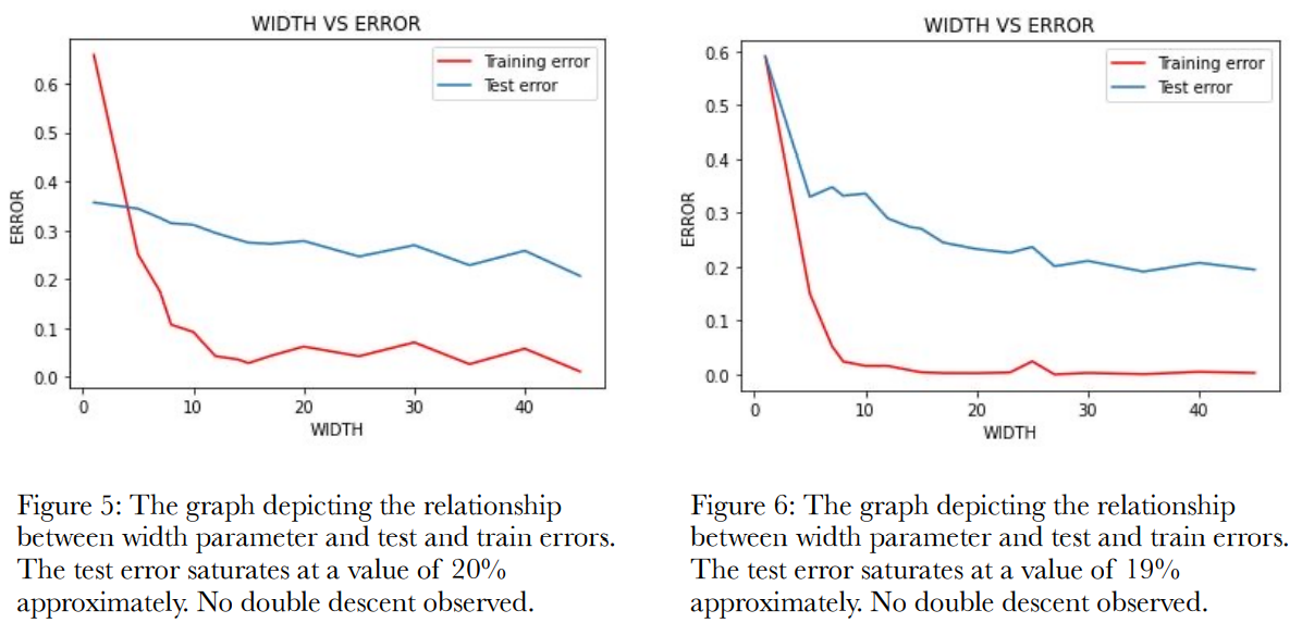
performances for the same number of epochs. The figure 5 and figure 6 show the performance with respect
to 40 and 400 epochs respectively, where width varies from 1 to 40. As one can observe here, there was no
concrete appearance of double descent even after 6 trials.
b. Varying the number of CNN layer
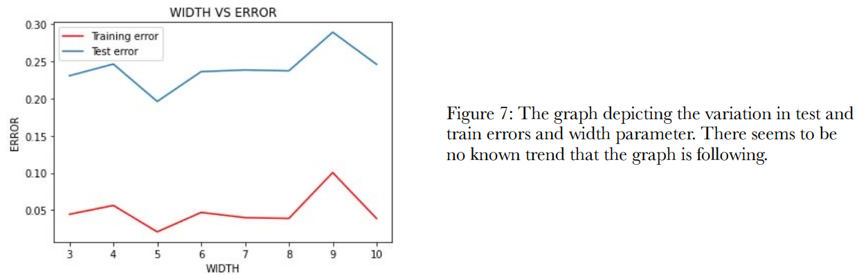
Here, we try to understand how the test and train errors vary with respect to the addition of more CNN
layers. The layers added are added with “same” padding and of the same width equal to 4c. The number of
epochs used is 400. The minimum number of CNN layers is 3 with widths [c, 2c, 4c]. The performance of
the model with respect to varying number of CNN layers is shown in the figure 7.
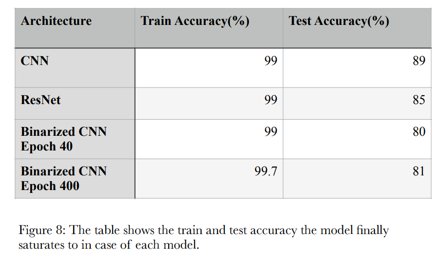
Given in the figure 8 is the table summarising what values of test and train error do the models saturate at
when the width parameter is varied.
Inference
To, draw any concrete conclusions from this study would be too soon. But several inferences can be drawn
including:
- Double descent does not show for lower number of epochs.
- The test error doesn’t follow any known trend when number of CNN layers is increased.
- BNN performed very effectively with the training set but not so much with the test one.
Future Work
The next stage of the study involves a comparative study between CNN and BCNN to formulate a
benchmark to predict the performance of a CNN architecture by training it’s corresponding BCNN on the
same datasets. For people with limited computational resources, it can be a good way of evaluating
architecture performance on their dataset in less amount of time and higher number of epochs. This study
would be based upon the observation the BCNN takes very less time in training for higher number of epochs
as compared to CNN.
References
- Preetum Nakkiran et al. (2019), Deep Double Descent: where bigger model and more data hurt?
- Itay Hubara et al. (2016), Binarized Neural Network
28 Dec 2022
Understanding Surface acoustic Waves
The surface acoustic wave(SAW) is an acoustic wave traveling along the surface of a material exhibiting elasticity. These waves are the modes of propagation of elastic energy along the surface of the solid, whose displacement amplitude undergoes exponential decay. The SAW devices were first discovered by Lord Rayleigh in 1885, hence, SAW is also called Rayleigh waves. The Rayleigh waves have longitudinal and vertical shear components that can couple with any media in contact with the surface. This coupling strongly affects the amplitude and velocity of the wave, allowing SAW sensors to directly sense mass and mechanical properties.
Here, in SAW devices we will confine ourselves to the surface acoustic waves observed in case of a piezoelectric solid. A piezoelectric solid is the one which possesses the unique ability to transduce mechanical stress applied on it, into the form of a current and vice versa. Transduction refers to the conversion of one energy into another. Here, this transduction of mechanical stress into electrical current in the piezoelectric material is called the piezoelectric effect.
Structure & Working of SAW Device
If one considers the basic structure of a SAW device, it constitutes a substrate topped by a layer of piezoelectric solid and then, two IDTs, i.e., the input IDT and output IDT. The structure is clearly illustrated in the figure given below.
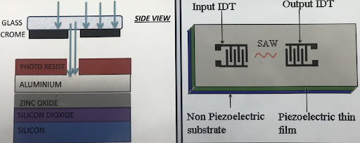
IDT stands for inter digital transducer. The IDTs are made using mono photolithography, which is discussed in detail later in the report. When an AC voltage is provided to the input IDT. The input AC voltage is converted to a form of surface acoustic wave, as the IDT is mounted on piezoelectric layer. The SAW propagates through the delay region to eventually reach the output IDT. The output IDT does the opposite of input IDT and converts the vibration applied to itself into an AC voltage. This voltage received is recorded and made sense out of in many of the SAW device applications.
The finger-like structure in the IDTs are actually electrodes made out of a metal. The metal used in the study for this purpose is Aluminum.
In the fabrication of SAW devices, ZnO is the piezoelectric solid used. One might ask why ZnO is used, there are other piezoelectric materials available like quartz, LiTaO3, LiNbO3, etc, as well. The answer lies in the layered structure of ZnO, which allows relatively higher SAW propagation velocity (5000 m/s). The other piezoelectric materials like quartz, LiTaO3, etc, show less SAW propagation velocity, i.e., in the range of 3000 to 4000 m/s.
In all honesty, diamond materials possess the highest SAW propagation velocity of about 11000m/s, but the poly-crystalline diamond layers grown by hot filament CVD process usually have very large grain size and rough surface, which requires a huge amount of mechanical polishing to improve surface smoothness to a level good enough to be used in the fabrication process of SAW devices (Ra~5nm). Such processes are very time consuming and expensive. Hence, we can strike off diamond materials from the list of piezoelectric solids that can be used. But if you are really not under the constraint of budget, there are nanocrystalline diamond materials which don’t require such post-polishing processes and can be used for fabrication of SAW devices. In the study mentioned, however, we stick with ZnO.
Fabrication Processes
A number of processes are carried out on a given substrate to fabricate a SAW device. In our study, as mentioned above we use two substrates. First is passivated silicon wafer. By the term “passivated”, we mean that there is a layer of Silicon oxide (SiO2) on the wafer, 2-4µm thick. The layer of SiO2 is said to be the ‘sacrificial’ layer.
The second substrate used is corning glass. Corning is the name of the company which produces this unique glass. The specialty of this glass is that it can withstand a temperature of 600°C, whereas other glasses can’t possibly tolerate such a high temperature, they might melt.
The processes involved in fabrication of a SAW devices are mentioned below sequentially:
- Sputtering
- Electron beam deposition
- Mono photo-lithography
- Developing
- Etching
- IV characteristics check
- Packaging
SPUTTERING
Sputtering, by definition, is the deposition of metal or a target material on a surface by using fast ions to eject particles of it from the target. It can also be seen as the plasma etching of target material. As we know from the design, we need a thin layer of ZnO on the substrate. This layer is achieved by using the process of sputtering. The sputtering is of various kind based upon how the fast moving ions are achieved. However, we have used RF sputtering to achieve the required results, i.e., 4µm thick layer of ZnO.
Theory of RF sputtering
Plasma is one of the four fundamental states of matter. It is formed when an inert gas, like Argon, helium, argon, etc., get ionized upon being subjected to a very high intensity electric field. In sputtering, plasma plays the major role of removing molecules from target material’s surface by transferring their own momentum into them. Ar+ is the ion used in the sputtering process.
Radio frequency is used to form the plasma. It is used to ionize the Argon, introduced into the system, which is a very significant step in the process of sputtering. These Ar+ ions then bombard the target material, getting attracted to the cathode(target). The cathode is generally cooled because sputtering generates heat. The target molecules then float around, and some of it lands on the wafer(anode), hence, the thin layer of the target material on the wafer is attained. The anode can be cooled or heated.
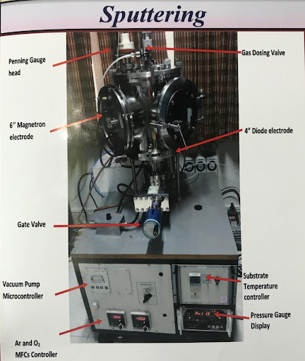
Process
The substrates used, must firstly undergo the cleaning process in order to remove most of the impurities from the substrates’ surface. The substrate is attached to the substrate holders using pins as shown in fig 1. This substrate holder is then placed inside the cylindrical sputtering chamber in an upright position. The target is labeled in the figure shown. The distance between the target and the substrate should optimally be 11.5cm. The chamber is then closed and the all the gas inlets are off.


All the air is vented out of the cylindrical sputtering equipment. The rotary pump is turned on in order to create a vacuum of the order of 10-2. Upon achieving the vacuum of the mentioned order, the turbo pump is turned on. The pumps are allowed to work till the vacuum of about 10-6 order is attained. This is done to assure that no air remains inside the chamber, which further ensures that no impurity pertains which may be able to strand or interfere with the process in any way.
One must know that it takes a significant amount of time to attain the vacuum level of 10-6 order. The time is generally 6 to 8 hours. So, one must equip patience while engaging in the process.
When the atmosphere inside the chamber is clean, the Argon inlet is opened, so as to allow the formation of plasma. The process takes place at about vacuum of order 10-2. The plasma once formed initiates deposition, as ionized argon molecules transfer their momentum to the target material and remove molecules. These molecules once freed roam freely in the chamber and some of them may attach to the substrate’s surface. Therefore, a thin layer of ZnO is deposited on the surface of the substrate. The time taken after the formation of plasma estimates to somewhere between 6 to 7 hours for proper deposition to occur.
ELECTRON BEAM DEPOSITION
Theory of E. Beam Deposition
The electron beam is concentrated on a target metal. This raises the temperature of the metal to the point of vaporization of the metal. Once the metal vaporizes it is made to conveniently condense on the wafer placed in vicinity. Hence, a thin film of metal is formed on the substrate’s surface.
Process
The substrate, after ZnO deposition, is loaded in an electron beam machine. Vacuum is created in the chamber to remove the chances of encountering impurities. The vacuum is created by using the backing and roughing valve. A very high vacuum is created, of the order 10-6 and a temperature of 100°C is attained.
The metal of choice is aluminum (Al). A thin film of aluminum is formed on the surface coated with ZnO. The metal is placed on a boat. The electron beam is focused on the metal. The metal first melts and then vaporizes. The vapor condenses on the substrate and hence a thin film of Aluminum is formed.

MONO PHOTO-LITHOGRAPHY
From this point forth in the fabrication of SAW, the substrate coated with ZnO and Aluminum will be called “work piece” for convenience, in the following report. The substrate surface is spin coated with photo-resist. The spin coating machine is effectively run for 1 minute at 1000 rpm. This forms a uniform coat of photo-resist on the surface of the substrate. One must remember that the process must be done in yellow light. The bonds of photo-rest are weaker with the substrate in yellow light.


After spin coating, the workpiece, already coated with photo-resist, is kept in the heater at a temperature of 90°C for half an hour. This is “pre-baking”. The heated workpiece is then placed under a mask aligner such that parts of the workpiece coated with photo-resist can selectively undergo UV exposure. The photoresist when exposed to UV rays, strengthens its bonds with the work piece. The mask plays a major role in the above process. The parts which are not supposed to be left covered with the photo-resist are not exposed to UV rays. The UV exposure is done for about 13 seconds. Note that the mask used is unique to the SAW device.


DEVELOPING
The workpiece, after being selectively exposed to UV rays, is then straightaway transferred to a developing solution. It is kept in the solution for 2 minutes. The developing solution is used to remove the photoresist from the parts of the workpiece, not exposed to UV rays. For example, the delay region. This is a crucial step because if not done carefully, the parts exposed to the UV ray will also have to part with their protective photoresist. The work piece is transferred to a microscope for checking, such that one makes sure that the sample is developed properly.


After development of the sample, it is kept at a temperature of 120°C for 20 minutes and then taken out for etching.
ETCHING
Etching is the process which can be described as the opposite of depositing. The Aluminum is supposed to be etched from the surface except from the electrodes of IDT. This is where the photoresist plays a major role. It protects the aluminum that forms the electrodes from getting etched.
The etchant is a solution containing potassium ferricyanide, potassium chloride and deionized water in the ratio 10:1:100. The work piece is dipped with the etchant and then, cleaned with deionized water. Etching is again a crucial process and should be done carefully. Aluminum is used to make the electrodes, as it is a very stable and conductive metal. Gold and Platinum have better properties than Aluminum, but they are highly expensive.

PACKAGING
The work piece is diced in order to isolate the devices on the wafer or the corning glass substrate. The device that resulted is of dimensions 1 cm and 0.5 cm and has passed the scrutiny of the checking process is then placed on a header and the contact pads on the device are connected to the contact pads of the header. This is done to establish an internal connection between the pins of the packaging and the actual device.
The device after the cap is put on the header, is input into a Vector Network Analyzer. The resultant is the graph depicted in the image given below.


In a Vector Network Analyzer, an electromagnetic wave is input into the device. The input electromagnetic wave is of the frequency range 50 to 150 MHz. The output wave is observed. The graph of gain and frequency is made and a number of observations are derived from it.
The frequency which is allowed to pass through our filter is given by the formulae,
where, F = frequency allowed to pass,
λ = acoustic wavelength
and v is given by the property of substrates.
One of the most significant observations is that our filter is able to filter a frequency of 98.18Mhz, as from the graph the loss is minimum in this case.
Conclusion
The fabrication of an Integrated SAW Device filter is complete. The filter is able to let an AC voltage of frequency 98.18 MHz pass through it. The SAW filters find their applications in a number of communication systems, for example, mobile/wireless transceivers, radio frequency and intermediate frequency filters, etc.